
NIT >> Newsletter
@NIT, Fall 2001
Director's Message
I hope that you have all had a great summer, and are now back at work with renewed energy and enthusiasm.
Elsewhere in this issue of our newsletter, you will see reports on some successful events we have held over the past few months, and a discussion of some events coming up in the near future. In my message, however, I would like to take this opportunity to welcome several people to our "NIT family".
Isabela Medina Rojas joined us recently as our receptionist/secretary. She holds a MASc in Environmental Engineering from the University of Toronto, and has extensive university and business office experience. She replaces Marjorie Boyle who is now working in the office of Research Services. Isabela is quickly getting the office well organized and updating our rapidly-growing list of NIT laboratory equipment. Please stop by the office to say hello if you have not already met her.
Dr. Henry Lee joined us in May as our Processing Lab Manager. He has a PhD in nuclear physics from the University of Toronto, and previously worked for many years at the Sudbury Neutrino Observatory. Although the prototype fabrication laboratory - one of the four NIT Open Research Laboratories being established in the new Bahen building - will not be operational for another year, anyone with experience in establishing a state-of-the-art clean room knows that a tremendous amount of time and effort is required to properly design and plan such a facility - especially one that will be used by many researchers with very different requirements for materials and processes. Henry has been doing a wonderful job in leading our planning activities and coordinating meetings between researchers, clean room consultants, university plant personnel, and building contractors. We will be selecting the contractor for the actual clean room design and construction from the finalists selected to bid on this job. Henry has also been working on the detailed specifications for the equipment to be installed in the clean room. If you wish to discuss the developing plans for this facility, please stop by to talk to Henry in room SF 4105B.
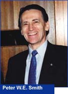
Professor Stewart Aitchison joined us in August as the new Nortel Institute Chair in Emerging Technologies. He comes to us from the University of Glasgow where he has been on their academic staff for over 10 years. Stewart was chosen from an outstanding list of international candidates by an inter-faculty search committee. He is internationally known for his work on nonlinear optics and optical solitons, and has broad research interests ranging from optical communications to planar silicon technology to biomedical optics and laboratory-on-a-chip technology. Stewart will also serve as the Thrust Leader for the Emerging Technology thrust, and is thus a member of the Program Committee. I look forward to his help and guidance in advancing our Institute programs and developing new initiatives in the years ahead.
Dr. David Maclean has been a key member of the NIT since its inception - indeed he was one of the architects of the Institute as it exists today. Up until recently, he served as the Nortel Networks on-site Manager. However, as a result of an internal Nortel Networks reorganization, the Manager responsible for the NIT is now Bruce Townsend. Bruce is stationed at Nortel Networks in Ottawa, and can be reached at (613) 763-3008 or by e-mail at townsend@nortelnetworks.com.
I am very pleased to announce that as of September 1, David Maclean will be serving us in a new role as the NIT Manager of External Relations. In this role, David will be responsible for providing initiative and expertise in implementing our strategy to expand existing partnerships and develop new relationships with industrial, university, and government partners to enhance our programs and to expand our resources and capabilities. The development of external partnerships to permit us to leverage our scarce resources and develop new programs is a key element of our strategic plan, and we are extremely fortunate that David, with his extensive experience and network of contacts, has accepted to serve in this new role.
As always, if you have comments or suggestions related to the NIT, please feel free to contact me at (416) 978-1646; pwes@ecf.utoronto.ca, or Helen at (416) 946-5176; hl.ni@utoronto.ca, Henry at (416) 978-8322; henryw.lee@utoronto.ca, or David at (416) 946.8058; dmaclean99@hotmail.com.
Nortel Institute Chair in Emerging Technologies Appointed
 The Nortel Institute is very pleased to announce the appointment of Prof. J. Stewart Aitchison as the new Nortel Institute Chair in Emerging Technologies, effective July 1, 2001.
When the Institute was established in 1997 by the University and Nortel Networks, it comprised a number of elements, including two endowed chairs and three new junior tenure-stream positions. The two endowed chairs were intended to attract the highest calibre of scholar and heighten the impact of the new Institute. NIT was very fortunate in the appointment of the inaugural Emerging Technologies Chair, Prof. Jimmy Xu, a recognized leader in semiconductor physics and optoelectronic devices and lasers.
To extend this short but solid tradition of excellence, Professor Aitchison was chosen from a strong list of international candidates. He received his BSc (with first-class honours) and PhD from Heriot-Watt University, Edinburgh, in 1984 and 1987 respectively. His doctoral thesis examined optical bistability in semiconductor waveguides.
From 1988 until 1990 he was a postdoctoral member of technical staff with Bellcore, New Jersey, where his research interests were in the areas of highly nonlinear glasses and spatial soliton propagation. From 1990 until recently, he was a member of academic staff in the Department of Electronics and Electrical Engineering, University of Glasgow, where he was Professor of Photonics.
The central theme of Prof. Aitchison's research at University of Toronto will be the application of optical technology to material processing, information technology and sensing applications. This will involve aspects of material processing, optical physics and biology. In particular, the use of optical technology to produce integrated optical circuits will be a key theme. (Photonics is the term which is used to describe the use of light to produce functional components, in the same way as "electronics" describes devices based on the use of the electron.) A number of discrete integrated optical components have been demonstrated, but currently there is no equivalent to the electronic integrated circuit. His research group will investigate the use of optical processing of III-V semiconductors, glass and polymers as a method for directly imprinting integrated optical components.
Prof. Aitchison also plans to investigate new materials in the quest for the optical equivalent of silicon. There has been an increasing amount of interest in the use of organic molecules for the production of low-cost optical components. These materials have been also been of interest in nonlinear optics because of the potential to engineer large values of second- and third-order nonlinear coefficients. However, the application of many of these materials has been limited by the difficulties involved in producing low-loss optical waveguides.
He will continue his work in spatial solitons, or self-guided beams of light, as a method of producing novel digital optical processing components. A spatial soliton can be thought of as a particle of light where the natural tendency of the beam to diffract is balanced by self-focusing, or self-lensing, in a nonlinear material. These particles of light can attract and repel each other, while solitons of different polarization can exchange energy. Such novel effects allow a range of all-optical signal processing elements to be imagined.
An area where photonics has a great deal of potential is in biological sensing, particularly when combined with micro- and nano-fabrication. Recent results have demonstrated that optical-based fluorescence can be detected from pico-litre volumes of nano-molar solutions. These techniques allow small-scale "lab-on-a-chip" components in which integrated optics provide an efficient and accurate diagnostic tool.
Prof. Aitchison will serve as the NIT Emerging Technologies Thrust Leader. "His broad experience in many areas of emerging technologies and his international research connections will be great assets for us," NIT Director, Prof. Peter Smith says. "We look forward to his leadership in strengthening and expanding our research program."
3-D Silicon Micromachined Components Enable Future Generation Broadband Satellite Communications
 The recent experience in satellite technology for personal communications (e.g., Iridium) clearly suggests that the commercial success of such systems critically depends on technologies capable of reducing the corresponding development and deployment costs. In addition, next generation wireless communications systems should be capable of supporting broadband data for "multimedia" type of applications. It can be argued that satellite communication technology, which can be made affordable to the average consumer and can support broadband information, can compete very successfully with existing or emerging terrestrial solutions. Indeed, satellite systems can offer the unique advantage of truly global coverage.
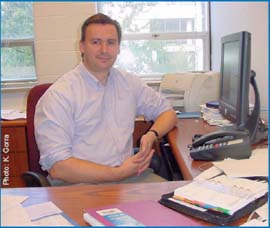
It is envisioned that in order to support broadband personal communications, the operating frequency of future generation satellite systems has to be increased to millimetre-wave (mm-wave) frequencies (loosely speaking 20-100 GHz). At this frequency range, low-cost printed circuit technologies become inadequate mainly due to increased conductor losses and reduced power levels from semiconductor devices. This makes the use of conventional low-loss metallic waveguide technology appealing for mm-wave front-end systems. Therefore, the task of developing low-cost hardware at mm-wave frequencies for broadband personal communications becomes even more challenging due to the high-cost associated with conventional machining. To this end, in a project Nortel Institute Associate George V. Eleftheriades and his colleagues, Ph.D. candidate Micah Stickel and Technologist Peter Kremer, are developing alternative low-cost waveguide technologies, based on silicon micro-machining techniques. The main advantages of this approach over conventional waveguide machining include the capability of batch processing based on standard photolithographic techniques, compatibility with integrated-circuit fabrication techniques, easy integration with semiconductor devices, implementation of lightweight components and natural scalability to increasingly higher frequencies.
At the present state of the project, a novel bulk silicon micromachining technique for fabricating millimeter-wave waveguide components has been developed. By adopting two-sided wet KOH etching of <100> oriented wafers it becomes possible to form deep, three-dimensional stacked structures in silicon of almost constant cross-section.
A crucial feature contributing to the success of this process is the ability of metallizing the stacked wafers after bonding. This post wafer-bonding metallization process reduces the effects of air-gaps and contact resistances arising when the wafers are stacked from the 3-dimensional silicon components. Furthermore, the developed process eases the wafer alignment task.
Another important aspect of the developed technology is that only conventional, low-cost, CMOS grade silicon wafers are required. This is in contrast to the common practice of other competing groups around the world which are employing non-standard, low-yield and expensive high-resistivity silicon wafers to produce micromachined circuits. With these innovations, it becomes possible to realize high-Q components at a low fabrication cost. These high-Q components can easily be integrated with electronics on the top wafer which can be silicon, GaAs or any other suitable microwave substrate to create complex 3-dimensional microwave integrated circuits. Such an approach holds promise for the implementation of low-cost, batch reproducible subsystems for broadband satellite (and indeed terrestrial) front-end communications.
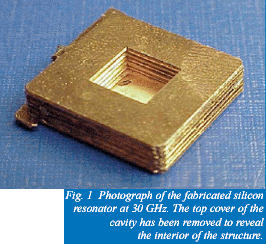
Recently, the developed fabrication procedure has been applied for the implementation of a silicon cavity resonator at 30 GHz. A photograph of the developed hardware is shown in Figure 1.
An unloaded Q-factor of 2155 has been measured which is, to Prof. Eleftheriades’ knowledge, the highest (by far) value reported to date for a bulk micromachined cavity at this frequency. The cavity resonator can be integrated with electronics to produce low-phase-noise voltage con-trolled oscillators (VCOs) or as a building block for the creation of waveguide filters and antennas, all inte-grated in silicon. The grand vision that we have is to micromachine entire satellite front-end subsystems in silicon, using the developed low-cost and batch reproducible micromachining techniques.
Prof. George V. Eleftheriades
NIT Associate
 Inaugural NIT Day a great success
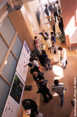
Over 90 researchers and graduate students involved with the Nortel Institute met on NIT Day on July 13, 2001, to learn more about the Institute and each other. Given the Institute’s interdisciplinary mandate, researchers associated with NIT are located across the University community, and this was a special opportunity for all of us to get to know one another better.
The schedule included a welcome by the Dean of the Faculty of Applied Science and Engineering, Tas Venetsanopoulos, an overview of the NIT by Director Peter W.E. Smith, and introductory talks by each of the NIT Research Thrust leaders. Poster boards were set up by the research groups.
To see pictures from the Day, click here
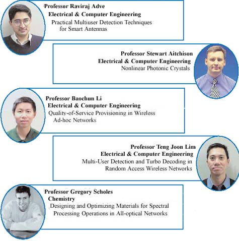
Five New NIT Associates announced
New NIT Processing Facility Manager
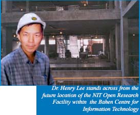 In May, the creation of NIT's Open Research Facility took an essential step forward with the appointment of Dr. Henry Lee as Processing Facility Manager.
Dr. Lee has a PhD from the Department of Physics at University of Toronto in experimental nuclear physics, specifically in ultrasensitive mass spectrometry using heavy ion beams from an accelerator. He comes to NIT from the Sudbury Neutrino Observatory (SNO) where he was Research and Development Co-ordinator. SNO is a leading research centre with a clean room environment, ultrapure water and gas systems and highly developed safety conscientiousness. It provides a multidisciplinary high tech research environment for engineers, physicists, chemists, biologist and technologists.
Initially, Dr. Lee is taking responsibility for the planning and equipping of the new clean room processing laboratory within the NIT Open Research Facility in the new Bahen Centre for Information Technology at the University of Toronto. When the Facility opens in 2002, Dr. Lee will be in charge of the laboratory, developing and expanding its role in research and development with university and industry partners. He will also participate in interdisciplinary research in collaboration with faculty, postdoctoral fellows and graduate students.
Dr. Lee says: "I am absolutely delighted to be working at NIT at this very exciting time and look forward to tackling the tremendous challenges ahead." The Processing Facility is a vital element of the Open Research Facility, fulfilling a key part of the Institute's mission to provide first-class infrastructure for university and industry researchers. With an area of 234 square metres, it will consist of two clean rooms with their associated change rooms and service rooms as well as a general-purpose work room. There will be a class 1000 clean room to house wet chemistry and photolithography functions and a class 10000 clean room to house the big machines for deposition and etching.
To date, Dr. Lee has been working on identifying equipment, laying out the placement of various elements and specifying all the services required for the facility. All the lab requirements have been drawn up into a proposal, which forms the basis for a competition among chosen design/build companies. NIT expects to select the winning design this Winter. We welcome Dr. Lee to our team.
Announcements
Nortel Institute for Telecommunications of the University of Toronto &
Edward S. Rogers Sr. Department of Electrical and Computer Engineering Distinguished Lecture Biomedical Imaging using Optical Coherence Tomography Imaging
Dr. James G. Fujimoto
October 26, 2001
Click here for details
Nortel Institute Undergraduate Scholarship 2001
Click here for details
