NIT >> Newsletter
@NIT, Spring 2003
Director's
Message
 In this issue of @NIT, we are featuring our Open Research Laboratories. These new facilities represent a major milestone in the development of the Nortel Institute, and they will provide the foundation for much of the program development that we will be undertaking in the coming years.
From a research perspective, these facilities are permitting the undertaking of larger and more ambitious projects than would normally be possible in a university setting. These facilities are currently being utilized for research in a wide variety of areas including studies of novel microwave and optical devices, metamaterials, organic and polymer materials and devices, and novel communication network architectures and management. The availability of these research facilities significantly assists the university in attracting and retaining top research professors and graduate students, and improves the quality of student training.
The Open Research Laboratory facilities are also serving as focal points for the development of partnerships with new industrial partners and with researchers from around the world. For example, we have recently submitted a proposal for a new research program enabled by the establishment of an agile photonic network testbed that would address the critical challenge of building a truly dynamic network using light - a network that responds independently to the ever-changing needs of the users. This program will elevate innovation in true photonic networks to a new level of excellence in Canada. It will unite researchers in photonics, systems and control, and communications at the University of Toronto, and will involve partnerships with both Nortel Networks and Corning.
A recent article in the University of Toronto Bulletin suggested that the key benchmarks for a great university are the three "I"s: innovation, indisciplinarity and internationalism. The NIT plays an important role in addressing all of these points.
Innovation is enhanced when close contact is maintained between basic researchers in the university, applied development in industry, and government programs for research support. The NIT, through our close connections with government and industrial partners is well situated to stimulate innovation. Our aim is to further develop our programs with the aid of the resources of the Open Research Laboratories by attracting additional industrial users and establishing new partnerships.
The NIT is organized to encourage interdisciplinarity. Because it is not situated within any single Department of the University, it is well positioned to coordinate cross-departmental and cross-faculty projects, and to take advantage of these collaborations to generate new multidisciplinary research proposals. One example is our recent development of a new research thrust in organic and polymer optoelectronics that involves researchers from several universities in the fields of physics, chemistry, and electrical engineering.
The NIT is involved in a number of international research collaborations. The organic and polymer optoelectronics thrust has strong ties with several research groups in France -- most notably the ENS-Cachan group of Prof. J. Zyss. Another major effort this year is an NIT workshop planned for this Fall with a delegation of Scottish representatives from universities and industries meeting with their Canadian counterparts for a series of technical sessions to explore and develop collaborations in areas of mutual interest.
In closing, let me summarize my message by stating that Nortel Institute is dedicated to establishing new partnerships. We welcome inquiries from interested parties and would be pleased to set up lab tours, meetings with key researchers, information sessions, etc to provide further information on the opportunities available.
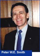
P. W. E. Smith
May, 2003
NIT celebrates official opening of the Open Research Facility
On May 30, 2003, the Nortel Institute for Telecommunications of the University of Toronto will be having the official “grand opening” of the NIT Open Research Facility.
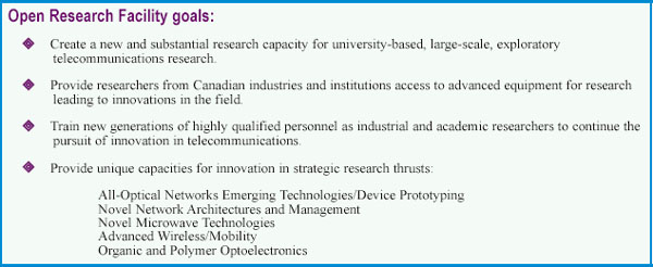
The first of its kind in Canadian universities, the NIT Open Research Facility is a large, open, integrated laboratory facility to support information technology and telecommunications research and training. It represents a new and substantial research capacity for university-based, large-scale, exploratory telecommunications research.
The Facility will be officially opened by University of Toronto President Robert Birgeneau together with key university, government, and industry stakeholders who have contributed to the Facility.
In addition to providing first-class research infrastructure, the Open Research Facility also provides a forum where NIT researchers and partners can meet and exchange information. This facility, with its specialized advanced equipment, will play a key role in training generations of highly qualified personnel to continue the pursuit of innovation in telecommunications.
 The Facility is a focal point for a multidisciplinary group of academic, government and industrial researchers. It consists of is a grouping of laboratories at the University of Toronto that includes a collection of equipment resources and technical expertise, enabling scientists from across academia, government, and industry to pursue research and development projects related to the research thrusts of NIT. These facilities are available to any researchers having need of the specialized equipment and operational expertise.
Building on more than two decades of outstanding achievement in collaborative research and education, the University and Nortel Networks created the Institute in 1997. One of the mandates of the Institute was to foster and accelerate research in select targeted areas of network, wireless and emerging technologies. To achieve this mission, the Institute boldly proposed the "Open Research Facility" as a key resource.
The Institute was successful in obtaining substantial funding from the Canada Foundation for Innovation (CFI), the Ontario Research and Development Challenge Fund (ORDCF) and the Ontario Innovation Trust (OIT). The CFI supports research excellence and helps strengthen research training at institutions across Canada by investing in research infrastructure projects. The OIT provides capital funding in support of research, while the ORDCF is designed to promote research excellence in the province by increasing the R&D capacity of Ontario universities and other research institutions through private and public sector partnerships.
With this funding, the Institute acquired extensive space for 10 laboratories (1100 square metres) distributed across the University of Toronto downtown campus. The labs are contained within the Bahen Centre for Information Technology (BCIT), Sandford Fleming and Pratt buildings.
The resources of the Facility are maintained by professional staff. The staff are not dedicated to particular research projects but are available to help users in the execution of their projects. The flexible nature of the facility, its equipment and staff, as well as its open structure, make it ideal for prototype development and testing. The facilities are open to University and industrial researchers who can use the facility to take advantage of its equipment and researcher expertise.
The NIT multidisciplinary, hands-on environment provides a valuable educational experience for the users. It provides an opportunity to interact in the laboratory with researchers from many different research fields and institutions.
The facility's funding supports only the lab infrastructure, equipment, and limited staff resources. Research projects in the facility are separately supported by industry and government agencies through the normal research grant mechanism.
NIT encourages interested researchers to discuss potential research collaborations and partnerships with the appropriate NIT Research Thrust Leader. Proposals to utilize the facility are reviewed to ensure high scientific standards and efficient use of this facility and are evaluated on an individual basis.
Antenna Test Labs
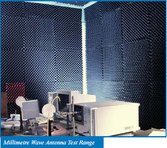 The antenna testing laboratories consist of two separate anechoic chambers fully shielded against electromagnetic interference. One chamber is lined with microwave frequency absorbing material and the second with millimetre-wave frequency absorbing material.
The Antenna Pattern Measurement Lab is a full anechoic chamber that operates in two frequency ranges: at lower microwave frequencies from 1GHz to 40GHz and in the millimtre-wave frequency range 34GHz to 75GHz. Antennae under test are mounted on a pedestal and antenna patterns are made using computer controlled positioners in azimuth and elevation. Absolute antenna gains can be carried out over both frequency ranges. In-house developed software is programmed to computer control the network analyzer, signal source and two axis positioner.
The Millimetre Wave Antenna Range enables swept-frequency measurements of amplitude as well as absolute antenna gains at millimetre-wave frequencies from 50GHz to 100GHz. Antennae under test are mounted on a rail on an optical table and antenna patterns are made using a computer controlled azimuth positioner.
RF and Microwave Testing Lab
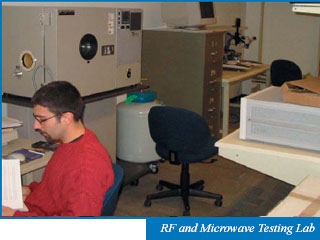 This is a state-of-the-art RF/Microwave testing lab that houses a complete set of RF, microwave and millimetre-wave sources, spectrum and vector network analyzers as well as a load-pull characterization facility. The testing lab enables coaxial as well as on-wafer probing and testing of devices and circuits.
Examples of devices and circuits that are characterized include metamaterial-enabled microwave devices, silicon micromachined and RF-MEMS devices, RF ICs and MMICs, and antenna input impedances. Current research includes millimetre-wave systems, integrated-circuit planar antennas and arrays, adaptive antennas, micromachined components, high-speed digital backplanes and interconnects, and the characterization and applications of novel electromagnetic materials.
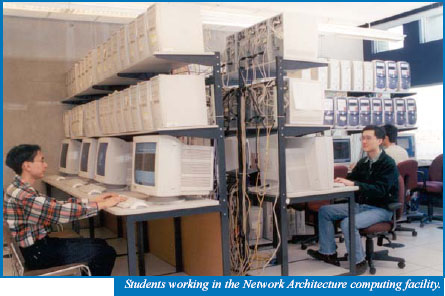
Network Architecture Labs
Encompassing research relevant to next-generation network architecture and future information services, the Network Architecture labs are being used to develop, test, and assess networking concepts that can form the basis of flexible, programmable, multi-domain network architectures to provide a platform for the delivery of a wide range of services. Ideally, this future generation network will combine the reliability of the existing telephone network, the flexibility of the Internet, the bandwidth of cable television networks, and the mobility of cellular radio.
The lab is equipped to facilitate the investigation of novel network-based applications and services, network architecture design, management and performance, heterogeneous networking, novel network elements, and network protocols and algorithms. An array of programmable end systems serves as a platform for the investigation of new applications (e.g., client-server, peer-to-peer, overlay networks). A complementary programmable node testbed provides the required network services and also provides a platform for the investigation of network architecture issues (e.g., signaling, security, QoS, routing).
The computing facility currently has 110 PC computers. The PCs run the Linux operating system to enable programmability of the network protocols. The computers are interconnected by a network of high speed layer 2/3 switches that allow the topology to be rearranged as required. One of the PCs is officially assigned as an access router to the ABone (Active Networks Backbone Testbed) with hostname, abone.nal.toronto.edu. This machine allows researchers to access an experimental testbed that is dedicated to active networking research in North America. The facility is being upgraded to support Windows applications as well as emerging communicating devices.
Device Prototyping and Fabrication
The Device Prototyping and Fabrication labs include: Organic Lead-Emitting Diode (OLED) Cluster Tools, Cleanroom/Prototyping, and Micromachine Etching labs.
 One lab contains Canada's first OLED cluster tools for molecular thin films and optoelectronics device prototyping. The cluster tools' unique capabilities help us leapfrog many other research groups into the forefront of this very competitive field. Indeed, the lab is quickly becoming a premier research resource in North America. Professor Zheng Hong Lu has assembled a unique set of investigative tools and techniques to study the fundamental science of cathode formation. He has developed important and innovative techniques such as in-situ cleaving at the cathode/organic interface to directly study the physics and chemistry at this interface.
The Cleanroom/Prototyping Lab enables researchers to fabricate functional devices in silicon, compound semiconductors, ceramic, glass and polymer.
The main laboratory consists of an 800 square feet Class 1000 (ISO 6) cleanroom for photolithography and wet chemistry. It houses two fully exhausted wet-chemical benches, laminar workstations, mask aligner and associated equipment for conventional lithographic process and the capability for developing novel patterning techniques. One of the first major pieces of equipment that has been installed is a Suss-Microtec MA6 mask aligner that will allow pattern transfer to photoresist-coated substrates.
The second cleanroom is a 480 square feet Class 10000 (ISO 7) for the etching and deposition machines such as e-beam thermal evaporator, chemical vapor deposition and reactive ion etching.
Finally, there is a 250 square feet “General Purpose” work area located outside of the cleanrooms with a six-foot long fumehood. This area is to be used for sample preparation and sample characterization.
The lab has its own dedicated heating, ventilation, air conditioning system (20C, 45% relative humidity) and dedicated exhaust system (for wet benches, fumehood, gas and chemical storage cabinets, vacuum pump exhaust, etc.).
The Macromachine Etching Lab is used to compliment other NIT laboratores. The function of this laboratory is to fabricate etched microwave circuits for printed antennas, metamaterials and microstrip circuits, and for micromachining of bulk silicon devices. The laboratory consists of a photoresist safe room with an exhausted fume hood and acid resistant work benches and wet benches.
Photonic and Optoelectronic Characterization Labs
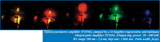
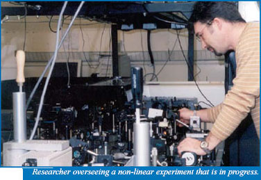 The photonic characterization laboratory is based on a tunable high-power, ultrashort-pulse laser system which can be used to characterize novel organic and polymer materials and devices over a wide range of optical wavelengths and power levels. Professors Ted Sargent and Peter Smith and their research teams provide the expertise on nonlinear and ultrafast measurement techniques.
Current applications include studies of optical nonlinearities and dynamical processes in semiconductors, semiconductor nanocrystals, and organic polymer materials. Versatile equipment and a unique suite of in-house developed diagnostic and analytical tools allow performing a broad range of nonlinear and time-resolved experiments.
The labs are also equipped for characterization of the optoelectronic properties of new materials and devices. A combination of low-noise current sources, monochromators, optical detectors spanning various wavelength ranges, and laser excitation sources allow a suite of experiments. Photoluminescence quantum efficiency, photoluminescence excitation, photoinduced absorption, and electroluminescence efficiency and spectra can all be acquired in the steady-state and with time resolution.
Announcements